In the top left corner, RX/TX are numbered in correctly, they are really digital 0 and digital 1, not 1 and 2.
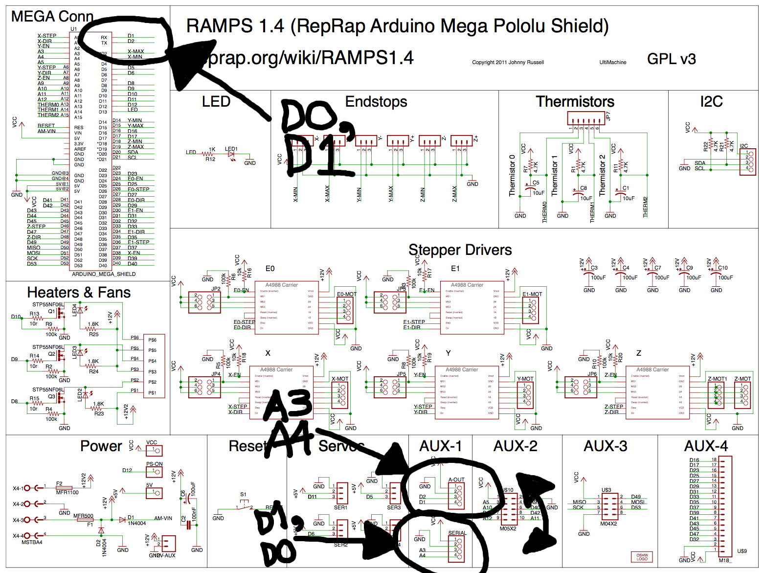
In the middle bottom, A-OUT and SERIAL connectors are basically swapped. SERIAL is really D0, D1 (the RX/TX mentioned above) and not A3, A4. And therefore A-OUT must really be A3, A4.
On the PCB, it's hard to tell which is A-OUT and which is SERIAL on AUX-1. The serial pins have tiny letters "s" next to them. This is the row of 4 towards the center of the board. A-OUT is the row towards the board edge.
Eric - I am sure that whoever did the documentation for the Mega 2560 and Ramps 1.4 was totally intent on confusing as many people as possible. I am sure they succeeded. Atmel labels the I/Os as Px# - I assume P is for Port, x is for the group and # is the sequential number. Then the Mega2560 schematic throws in the functions for the pins so you have PE0(RXD0/PCIN8) and PE1(TXD0). Of course that translates to RX0 and TX0 that go to the PWML connector pins 1 & 2 that are labeled PWML 0 & 1 and they are then designated as part of the COMMUNICATIONS connector on the silkscreen. The Ramps board then shows them as simply Rx & Tx and designates them D1 & D2. They then proceed to label them D0 & D1 for the physical board, and seal it by inverting the label. I'm still trying to figure out how A3 & A4 are D57 & D58 also. Then of course it is obvious that A3 is actually ADC3 on the schematic, and ADCL is the left Analog Input connector. Don't you just love consistency?
ReplyDelete